
Cart is empty

Curabitur placerat magna sollicitudin
NAND Flash Programming
Technical Guide Contents
This article describes how to program NAND Flash devices using a Xeltek universal programmer. Before reading this article the user should know certain keywords such as
block, ECC, main area and spare area which are used in NAND datasheets.
1. An introduction to NAND Flash
For most NAND flash chips, there are 512x8 (or 256x16) or 2048x8 (or 1024x16) bits in the “Main area," and 16x8 (or 8x16) or 64*8 (or 32x16) bits in the “Spare area" for a total of 528x8 (264x16) or 2112x8 (or 1056x16) bits per page. A block consists of many pages, but because the “Spare area" is reserved for bad block mark and ECC values, only the “Main area" is available to the user. For a 2-Gbit NAND device, it is organized as 2048 blocks, with 64 pages per block (Figure 1). Each page has 2112 bytes total, comprised of a 2048-byte data area and a 64-byte spare area.
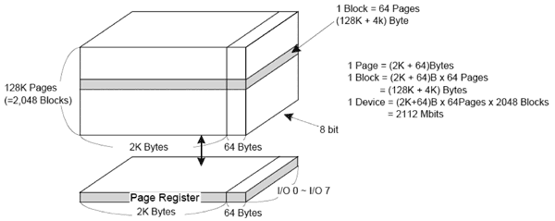
Figure 1
NAND flash devices hold the advantages of large capacity with low cost compared to NOR FLASH devices. In addition, NAND's advantages are fast write (program) and erase operations while NOR's advantages are random access and byte write capability. NOR's random access ability allows for execute in place capability, which is often a requirement in embedded applications. The disadvantages for NAND are slow random access, while NOR is hampered by are slow write and erase performance.
NAND is better suited for file applications. However, more processors include a direct NAND interface and can boot directly from NAND (without NOR).
NAND is similar to a hard-disk drive. It's sector-based or page-based and suited for storing sequential data such as pictures, audio, or PC data. Although random access can be accomplished at the system level by shadowing the data to RAM, doing so requires additional RAM storage. Also, like a hard disk, NAND devices have bad blocks, and require error-correcting code (ECC) to maintain data integrity.
The NAND flash may include invalid blocks when they are first shipped. Additional invalid blocks may develop while being used. Invalid blocks are defined as blocks that contain one or more bad bits. Erasing and programming factory-marked bad block are prohibited.
Bad blocks have been initialized before shipping and marked in the specific area. New bad blocks can be generated during usage so the system will have to identify these blocks.
Bit inverse is easier to find in NAND flash. If bit inverse happens in the important file, it will cause a system shut-down. Therefore, ECC/EDC algorithms are suggested for reliability when programming NAND Flash.
2. How to handle the bad blocks
There are many methods to handle the bad blocks. The customer can choose a method according to their own requirements or ask Xeltek to customize the algorithms for their own solutions.
To handle the bad blocks in the embedded system, an extra “layer" of software is required. Therefore, to program NAND flash chips, all we need to do to handle the bad blocks is to treat them in exactly the same way as they are handled by the user's system. As simple as this may sound, there are many ways to do this and there doesn't seem to be any universally accepted standard method.
For example, one common method is to just skip over the bad blocks and place the data in the good blocks. We call this the Skip Block Method. Another common method (by Samsung) is to allocate some of the blocks as a “Reserve Block Area." In this area, one block is used for a “table," that keeps track of the bad blocks and the rest are used for the data that would have been written to the bad blocks. Both methods are contained in our current base algorithm for NAND flash.Currently, we have 5 to 6 methods to handle the bad blocks. Two common methods are illustrated here.
2.1 Skip bad block
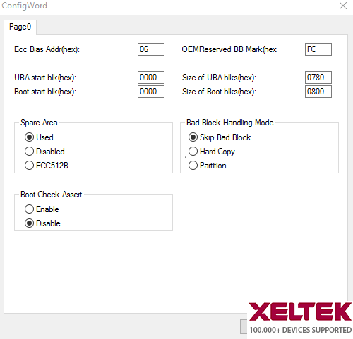
Figure 2
Block Area RBA: Reserved Block Area. The user can select programming mode by setting “ConfigWord."
Note: If the user's data includes “Spare data," please look at the addition sector about new method.
The skip bad block method is the simplest and most common method. It is very straightforward. It just skips over the bad blocks and places the data in the good blocks. The algorithm checks the block by reading the bad block mark. When the target address corresponds to a bad block address, these pages are stored in the next good block, skipping the bad block. Because this bad block is skipped, the original factory programmed (non-FFh) data in the spare area indicating the presence of the bad block is still there. Therefore, the user's system can also build a table of bad block addresses by reading the spare area of all the blocks at boot time.
Because the bad blocks exist, the size of user's data should not exceed the size of good blocks. Please, Fill the correct value in the “UBA start block" and “Size of UBA blocks."
Some NAND devices are available with all blocks being good. The user can also use the device without any bad block by filling max value in “Size of UBA blocks."
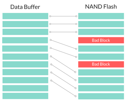
Figure 3
Using this method, the customer needs to check User Block Area (UBA) start block?Size of UBA blocks in the figure 2. The Reserved Block Area (RBA) start block and the size of RBA blocks are used for reserved block method. Boot start block and Size of Boot blocks are used to check if there are bad blocks used in boot area.
UBA start block shows the staring address to program the chip. The default address is 0000. The size of UBA blocks is the number of blocks to be programmed.
2.2 Reserved block
In this method, a mapping table will be generated. When a bad block is identified, the software will reserve a good block to replace it and create a mapping table saved in a reserved area.
When a bad block is detected during reading a chip, software will read the mapping table and then read the replaced block. The advantage is that the storage area has logical integrity. When an error happens in Block A, try to reprogram the data into another Block (Block B), by loading from an external buffer. Then, prevent further system accesses to Block A by creating a bad block table or by using another appropriate scheme. This is called “Block Replacement."
The programming algorithm works by first determining which blocks will be used as the User Block Area (UBA) and which blocks will be used as the Reserved Block Area (RBA). The starting address and size of the UBA are determined by the parameters entered in “UBA start block" and “Size of UBA blocks." Also, the starting block and size of the RBA is defined by the user as well.
Between the starting address of UBA and RBA, there are some blocks reserved for replacing the bad blocks.
The algorithm reads the spare area of the device, and constructs a “map table" in the RBA. Only the first and second valid blocks in the RBA are used for this table.
The map table contains information on how to substitute bad blocks in the UBA with good blocks in the area reserved for placement. The data fields in the map table are shown below.
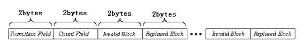
The Transition Field is always FDFEh. The Count Field is incremented by one for each page of the map table. For the current algorithm, there are only two pages used so the field will contain 0001h for the page in the first block and 0002h for the page in the second block of the map table.
The data pair Invalid Block / Replaced Block shows the address of the bad block and the address of the replacement block respectively. The rest of the page consists of these data pairs. Since there are 512 bytes, the maximum number of data pair entries is 127. Usually this will be sufficient since the number of bad blocks is typically less that 1% of the total number of blocks for new devices being programmed. Of course, new bad blocks can be generated during usage so the system (using this method) will have to identify these blocks and update the map table.
The second page of the map table is used to duplicate the information in the first page in case one of these pages becomes corrupt during usage. All fields use “little endian" protocol; the low byte is first.
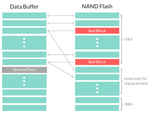
Figure 4
In figure 4, UBA is User Block Area. RBA is Reserved Block Area.
Reserved for Replacement Between the starting address of UBA and RBA, there are some reserved for replacement blocks used for replacing the bad blocks.
2.3 Write over bad blocks
This method is used to read all the data from NAND device to the buffer without considering bad block handling schemes. Therefore, the buffer also contains the data in the bad blocks. The customer can use other specific software to analyze the useful data by finding the locations of bad blocks. It is very useful if the NAND device was programmed by a third programmer.
2.4 Partition
Partition is used for NAND programming based on a partition table. A partition table is loaded and edited before programming, shown in Figure 5 and Figure 6.
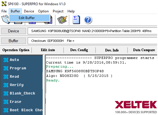
Figure 5
Figure 6
In the partition table, every 16-byte represents a partition, in which the bytes from 1
st to 4th represents the starting block address, the bytes from the 5th to 8th represent the ending block address, the bytes form 9th to 12th represent the block size actually used, the bytes from 13th to 16th is the conserved bytes. The address searching will end until the starting address is FF FF FF FF. The skip bad block method is used during programming. For example, there are three partitions need to be programmed for this chip. The starting address and the ending address for the first partition are 0000 and 007F. The actual block size is 0001.
3. Spare area in NAND Flash
If user's file includes the spare data, this method is valid. The algorithm will check the value of the bad block flag in the 1 st and 2nd pages and change the non-FF to FF value.
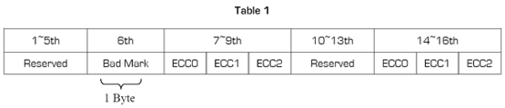
About the usage of Spare Area, we need to set the Spare Area (ECC) in Figure 2. If the file for programming includes Spare Area information, please select “Used". This setting should be used when the original data file contains information for the entire device, including the spare area. If there is no Spare Area information in the file for programming, please select “Reserved, ECC disabled". When you select “Reserved, ECC enabled", the original data file does not contain spare area data, but the user wants the device spare area to be programmed with ECC and/or other dynamic data. You will use the ECC algorithm generated by the software. The default algorithm used by our programmer is 512B ECC algorithm. Table 1 shows the format.
3.1 Selecting ECC
If “ECC" is selected, the algorithm will calculate three bytes of ECC data corresponding to the 512 bytes of data in each page. The ECC bytes are placed in the 14th, 15th, and 16 th Byte (with the copy in the 7th, 8th, and 9th Byte) location of the spare area (for example: byte 526, 527, and 528 of each page) as shown in Table 1.
If you want the SuperPro programmer to calculate the data for saving to Spare Area, please tell us the requirement in details.
3.2 Bad block mark
In general, the bad block mark for large page mode is in the 2948 byte of every block and in the 517 byte of every block. Therefore, the content of the bad block mark in the programming file is FF. If you didn't use standard processing method in your file, please contact us. We will customize the algorithm according to your requirements.
4. Boot blocks checking
The boot code must reside in good blocks because most systems can't handle bad blocks at boot – the code hasn't been loaded yet. The user can specify both the starting block for the known good area and the size by filling the parameters in the “Boot start block" and “Size of boot blocks".
During device programming, if a bad block is encountered in this range of blocks, programming reports error message at the end. The probability of failure increases when a larger number of blocks are used for a “known good area". We recommend that the minimum number of known good blocks be set aside for the boot code.
Generally, bad blocks are not allowed to reside in boot. Therefore it is necessary to check if there are bad blocks in boot. When programming NAND chips. If your boot area is in the first block, there is no need to check the bad block since most NAND manufacturers guarantee that the first block is good. Therefore, if your boot code can fit into a single block (and you specify a known good range of 1 block with a starting address of 0), you will not have any failures due to bad “boot blocks" during programming.
Figure 2 show the boot configuration. Boot start block shows the starting address of boot area. Size of Boot blocks is the size of boot area. Size of Boot blocks is set to be the size of all blocks in order to check all bad blocks of the Nand chip.
5. Programming
Programming the device will always write the ECC values in the “Spare area." Verifying and Reading the device will depend on ECC selecting. Blank-Checking and Erasing the device will operate on the all blocks. To avoid damaging the bad blocks marks, Blank-Checking the block is always done (Erasing when necessary) before programming it.
We suggest the user checking the ID of device, adding “Program" and “Verify" into “Auto" when programming the device. Because the size of NAND flash is very large, it will spend time at selecting the device, loading the file and executing first time.
Regarding support for new programming mode, file system and specific information of spare area,
please provide the detail description about your development requirements.
6. FAQ
If the NAND flash has been programmed by third party programmer, we can read the chip straight without consideration for good or bad block by checking “Write over bad blocks" in the Device Config. This method is used to read all the data from NAND device to the buffer without considering bad block handling schemes. Therefore, the buffer also contains the data in the bad blocks. The customer can use other specific software to analyze the useful data by finding the locations of bad blocks.
Random access of data in NAND flash is not possible and data can only be accessed serially. If a particular memory page is opened, data can be read easily and quickly. Commands should be sent serially to NAND flash interface (ONFI), making direct interfacing with NAND difficult. NAND Controllers makes it easier to access NAND flash and present the user with a clean, usable interface to the memory. Controllers also support optional error correction code (ECC) that performs single-bit error correction.
Multi-level cell (MLC) NAND flash stores two or more bits of information per memory cell, compared to one bit per cell for Single Level cell (SLC) NAND. MLC NAND has a larger capacity, lower cost/bit, slower and less robust. SLC = 100,000 erase/program cycles. MLC=10,000 erase/program cycle. MLC needs 4 bit ECC whereas SLC needs 1 bit ECC.
Large block=> (2048 bytes of data +64 byte of spare data) per page.
Small block=> (612 bytes of data +16 byte of spare data) per page.
Command sequences are different for large block and small block NANDs.
In large or small block NAND, there is 16 or 64 bytes of spare data in each page. Spare areas are used for storing ECC and other bad block management info (bad block mark).
Not all memory cells are fully functional in a NAND device. Some blocks (1 block = 64 pages) are declared as bad blocks. During testing, bad blocks are marked in spare areas of the first 2 pages of NAND flash. User should read bad block marks and avoid using them. Due to repetitive use of NAND flash, additional bad blocks may be created and user should also handle new bad blocks.
NAND Flash can be erased and programmed only for a limited time. If a page is accessed often , memory cells in that page can be damaged and thus failing the whole NAND flash. Wear leveling is used to balance NAND usage and distributes the memory usage evenly across all pages in a NAND device. This helps increase NAND flash life. It involves mapping of logical address to different physical address in the NAND device.
Duplicating a NAND flash is difficult if the target device already has some bad blocks. Copying a NAND flash is different than copying any other EEPROM or flash chips because bad blocks exist in NAND flash chips. For example, if the K9F1G08U0A NAND flash has been programmed by a third party programmer, we can read the chip straight without worrying about good / bad blocks by checking “Write over bad blocks/hard copy" in the Device Config. This method is used to read all the data from NAND device to the buffer without considering bad block handling schemes. Therefore, the buffer also contains the data in the bad blocks. This method is not recommended for large production as many target chips will have bad blocks.
As your NAND flash has been programmed by a third party programmer, chip-copy operation should be done by hard copy which can be subdivided into two steps – reading original device and programming target device.
- Reading original device: we can read the chip as it is without worrying about good or bad block by selecting “hard copy" in the Device Config. This method is used to read all data from a NAND device to the buffer without considering bad block handling. Therefore, the buffer also contains the data in bad blocks.
- Programming target device: The successfulness of programming operation can be hindered by bad block(s) occurrence in target device. Therefore, target device must be free of bad blocks. The number of bad blocks could be checked by enabling boot check assert in config word field. For doing this, please fill Boot Start Block with 0000, and Size of Boot blocks with total blocks (800). Click Boot Block Check in the software panel, Number of bad blocks will show. Using the hard copy method of duplicating NAND for mass production is not recommended. Please let us know if you can provide actual data file to be programmed along with more details such as information about spare area and bad block handling method to be used.
For NAND flash greater than 2GB, we recommend SuperPro 7500 programmer. SuperPro 7500 programmer supports files up to 256 GBytes which is more suitable for high density NAND flash chips.
In configword field, please fill Boot Start Block with 0000, and Size of Boot blocks with 2000. Click Boot Block Check in the software panel, Number of bad blocks will show.
ECC Error: ECC values are different with the devices
Good blocks not enough: User's data is larger than the size of good blocks.
RBA fails: A RAB value error can't read or verify.
Boot fails:
A: Not enough good boot blocks.
ECC_CORRECTABLE_ERROR
A:
Find ECC_CORRECTABLE_ERROR bit and correct.
Q: The default settings for the device configuration had the size of UBA Blocks set to 1F00, it also had RBA block size set to 0010.When using these settings we do not see the last 256 blocks. We are not using any type of Reserved Block area so I set the UBA Block size to 0X2000 and all other settings to 0, and selected Skip Bad Blocks. The SuperPro 3000U eventually gives me a "Good blocks not enough" error.
A: If you want to read all area of the chip, please first check bad blocks.Then subtract it from All-blocks. This is the actual blocks you want read.
Q: Config Error, not allow continuing operation
A: The problem happens because the variables in Dev. Config are not set properly. Correct setting is:
UBA start block < All Blocks, Size of UBA blocks <= (All Blocks - UBA start block)
Boot start block < All Blocks, Size of Boot blocks <= (All Block - UBA start block)
Under Reserved mode:
UBA start block < RBA start block, Size of UBA blocks < (RBA start block - UBA start block)
All Blocks > RBA start block > (UBA start block + Size of UBA blocks)
Size of RBA blocks < (All Blocks - RBA start block)
When copying a 16GB full device, SuperPro 7500 will read full size data with open ended read command from 0 to 16GB sector numbers.Then do data analysis before programming. Data analysis can split the 16GB data into data which needs to be programmed (non zero) area and data that does not need to be programmed(zero) area and make a partition table. So Programing procedure will read the partition table and write data which is needed to be programmed and skip data which does not need to be programmed.This will decrease programming time remarkeably. There will be a stop transmission and Check CMD status after every continue area.
Do you have any questions?


