
Cart is empty


Curabitur placerat magna sollicitudin
Device Configuration Settings for NAND Flash Programming
Xeltek SupePro 6100 and SuperPro 7500 support high speed programming of high density Nand Flash devices. For nand flash devices, the configuration word must be properly set before programming to ensure that the chip can be used on the target system. Most of the Nand flash chips have configuration word as shown below:
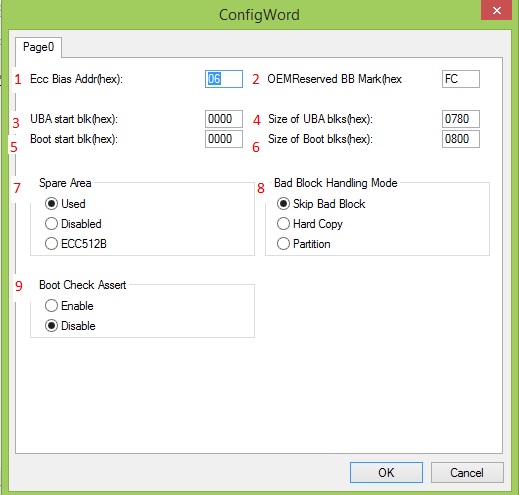
- ECC Bias Addr (hex):
ECC bias address [06] means indicates a bad block mark. For NAND Flash (8bit), the bad block mark is usually saved in 6th byte on the first and second page of each block. ECC Bias Addr exists in some old NAND chip settings such as (2048+64)bytes per page and is not useful for new chips. Leave in default settings. - OEM Reserved BB Mark(hex):
According to NAND datasheets, the BB mark is 0x00H. However, BB mark is different than OEMreserved BB mark and is defaulted to FC. OEMReserved BB Mark exists in some old NAND chip settings such as (2048+64) bytes per page. Leave in default settings. - UBA Start blk (hex):
User Block Area starting address or first address from where user's data starts. It is generally set to 0000h. - Size of UBA blks (hex):
The size of UBA (User Block Area) blocks is the number of blocks to be programmed.
MAX Size of UBA Blocks = All blocks - bad blocks.
Because bad blocks exist, the size of user's data should not exceed the size of good blocks. Fill correct value in the “UBA start block" and “Size of UBA blocks." If less number of blocks are programmed, programming timing is much faster. - Boot Start blk (hex):
Boot start block shows the starting address of the boot area. The boot code must reside in good blocks because most systems can't handle bad blocks at boot. - Size of Boot blks (hex):
Size of Boot blocks is the size of boot area. Boot start block and Size of Boot blocks are used to check if there are bad blocks used in boot area. Size of Boot blocks is set to be the size of all blocks in order to check all bad blocks of the NAND chip - Spare Area:
“Spare area" is reserved for bad block mark and ECC values. Only the “Main area" is available to the user.
If user data includes “Spare data", then select Used or disabled.
If there is no Spare Area information in the file for programming, select “disabled"
When user wants the spare area to be programmed with ECC and the original data file does not contain spare area data, select “ECC512B". This method uses the ECC algorithm generated by the SuperPro software. The default algorithm used by our programmer is 512B ECC algorithm. Contact techsupport@xeltek.com if user need to use other ECC algorithm. - Bad Block Handling Mode: Xeltek NAND programming algorithm provides three bad block handling methods:
- Skip Bad Block
It is most simple and common method. It skips over the bad blocks and place the data in the next good block. - Hard Copy
If the NAND flash has been programmed by a third party programmer, Xeltek SuperPro can read the chip without worrying about good / bad blocks by checking “Write over bad blocks/hard copy" in Device Config. This method is used to read all the data from NAND device to the buffer without considering bad block handling schemes. Therefore, the buffer also contains the data in bad blocks. This method is not recommended for large production as many target chips will have bad blocks. - Partition
Partition is used for NAND programming based on a partition table. A partition table is loaded and edited before programming. We can provide a tool to merge several files to one programming file and also generate a partition table file. When partition method is used, it actually uses skip bad block method to help avoid data overlap from one region (partition) to another just like a hard disk drive.
- Skip Bad Block
- Boot Check Assert
Boot Check Assert Enable means when a bad block is found in the range of 'Boot start block blks and size of Boot start block blks', the programmer will stop programming with an error of 'boot check fail'.
Few NAND chips may also have the following settings
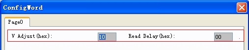
V adjust helps to change read voltage. If V Adjust is set to
0xf then read voltage is 1.6V
0x10 then read voltage is 1.7V
0x11 then read voltage is 1.8V
Read delay aims to change period byte in the read process.
Generally, it is not needed to change these settings.
Do you have any questions?


